

Here i discus on half adder and full adder circuit with truth table, block and circuit diagram.
Half-Adder
As the name suggests half-adder is an arithmetic circuit block by using this circuit block we can be used to add two bits. As we know it can add two bit number so it has two inputs terminals and as well as two outputs terminals, with one producing the SUM output and the other producing the CARRY.
For half adder circuit the relation between input and output expressed by the Boolean expressions for the SUM and CARRY outputs and it expressed by the equations bellow
SUM S = A^.B+A.B^
CARRY C = A.B
In bellow figure shows the truth table of a half-adder, showing all possible input combinations and the corresponding outputs along with block and circuit diagram.

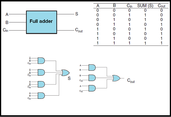
Full Adder
As we read early half adder can add only two bit of numbers so if we want to add two bit of input along with carry then we have to add three bits. But in half adder we can add only two bits so we need some extra. A full adder circuit is an arithmetic circuit block that can be used to add three bits to produce a SUM and a CARRY output. By using full adder we can add large numbers because it can add two bit number with carry. Let us recall the procedure for adding larger binary numbers. We begin with the addition of LSBs of the forward to the next higher column bits. As a result, when we add the next adjacent higher column bits, we would be required to add three bits if there were a carry from the previous addition. We have a similar situation for the other higher column bits also until we reach the MSB. A full adder is therefore essential for the hardware implementation of an adder circuit capable of adding larger binary numbers. For half adder circuit the relation between input and output expressed by the Boolean expressions for the SUM and CARRY outputs and it expressed by the equations bellow
S = A^B^Cin +A^.B.C^in +A.B^Cin^ +A.B.Cin
Cout = A.B+B.C+A.C
In bellow figure shows the truth table of a half-adder, showing all possible input combinations and the corresponding outputs along with block and circuit diagram.


1 thought on “Half adder and Full adder circuit”
I need a detail about microwave communication