The most interesting thing in 8085 microprocessor is interfacing memory chips with 8085 microprocessor. Because we know that 8085 microprocessor does not have any internal memory chip. So we have to interface it externally. Before entering main discussion we have to know answers of some questions.
- What is address space and address space partitioning?
- How can we generate of Control Signals for Memory?
- Example of interfacing.
What is address space and address space partitioning?
It is defined as the set of all possible addresses that a microprocessor can generate. 8085 microprocessor has a 16-bit address bus so that it can address 216 or 64 KB of address. It called the address space of 8085. This total address space can be partitioned or allocated to memory or I/O devices so that they can be addressed properly. This is called address space partitioning.
We know 8085 has 16 address lines (A0 – A15). Hence a maximum of 64 KB (= 216 bytes) of memory locations can interfaced with 8085 microprocessor. The memory address space of the 8085 takes values from 0000H to FFFFH. Hear H denoted for Hexadecimal number.
Another things we should know that the 8085 initiates set of signals such as IO/M, RD and WR when it wants to read from and write into memory. Similarly, each memory chip has signals such as CE or CS (chip enable or chip select), OE or RD (output enable or read) and WE or WR (write enable or write) associated with it.
Generation of Control Signals for Memory
Now come to the main part when the 8085 wants to read from and write into memory, it activates IO/M, RD and WR signals as shown in Table.
Table shows the status of IO/M, RD and WR signals during memory read and write operations.
And interestingly microprocessor 8085 itself using IO/M, RD and WR signals, two control signals MEMR (memory read) and MEMW (memory write) are generated. Fig. 1 shows the circuit used to generate these signals.
When is IO/M high, both memory control signals are deactivated irrespective of the status Of RD and WR signals.
Now it will be very helpful to us if we discuss an example. For that we take an example to elaborate the mater.
Example of interfacing.
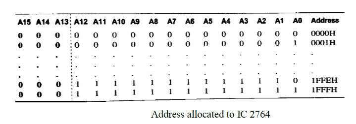
Ex: Interface an IC 2764 with 8085 using NAND gate address decoder such that the address range allocate to the chip is 0000H – 1FFFH.
Specification of IC 2764:
- 8 KB (8 x 210 byte) EPROM chip
- 13 address lines (213 bytes = 8 KB)
Interfacing Process :
- 13 address lines of IC connected to the corresponding address lines of 8085.
- Remaining address lines of 8085 connected to address decoder formed using logic gates, the output of which is connected to the CE pin of IC.
- Address range allocated to the chip shown in Table 9.
- Chip can enabled whenever the 8085 places an address allocated to EPROM chip in the address bus.
Hope the discussion clear your concept on interfacing memory chips with 8085 microprocessor.
Let’s check how you learn data transfer schemes of 8085 microprocessor with a simple quiz.
0 of 5 questions completed Questions: Data Transfer in 8085 microprocessor. You have already completed the quiz before. Hence you can not start it again. Quiz is loading... You must sign in or sign up to start the quiz. You have to finish following quiz, to start this quiz: 0 of 5 questions answered correctly Time has elapsed You have reached 0 of 0 points, (0) The control signal used to distinguish between an I/O operation and memory operation is The stack and the stack pointer The total I/O space available in 8085 if used peripheral mapped I/O The interfacing device used with an output port is In 8085 CPU, the JUMP instruction address affects theData Transfer
Quiz-summary
Information
Results
Average score Your score Categories
1. Question
2. Question
3. Question
4. Question
5. Question
You may read those too…..


1 thought on “Interfacing memory chips with 8085”
Pl. arrange group/ section for notes.