

In peripheral mapped I/O interfacing, the I/O devices treated as differently from memory chips. In this method the control signals I/O read ( IOR ) and I/O write ( IOW), which are derived from the IO/M, RD and WR signals of the 8085, are used to activate input and output devices, respectively.
Generation of these control signals
Now question is how this control signal generated?
Generation of these control signals shown in Fig. bellow. As well as table shows the status of IO/M, RD and WR signals during I/O read and I/O write operation.

In peripheral mapped I/O interfacing, IN instruction used for accessing input device. And OUT instruction used for accessing output device. Each I/O device is identified by a unique 8-bit address assigned to it. Since the control signals used to access different input and output devices. and we know thatt all I/O devices use 8-bit address. So maximum of 256 (28) input devices and 256 output devices can interfaced with 8085.

Explanation with Example
Now it will better for us if we discuss the topic with an example. In bellow we take an example and discussed to show how peripheral mapped I/O interfacing work.
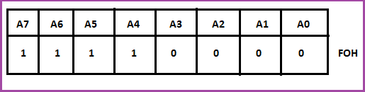
Ex: Interface an 8-bit DIP switch with the 8085 such that the address assigned to the DIP switch if F0H.
As per our above all discussion we know that in peripheral mapped I/O interfacing, IN instruction used for geting data from DIP switch and store it in accumulator. Steps involved in the execution of this instruction are:
- Address F0H placed in the lines A0 – A7 and a copy of it in lines A8 – A15.
- Activate the IOR signal ( IOR = 0), which makes the selected input device to place its data in the data bus.
- The data in the data bus then read and store in the accumulator.
Fig. shows the interfacing of DIP switch.
A0 – A7 lines are connected to a NAND gate decoder such that the output of NAND gate is
The output of NAND gate is ORed with the IOR signal and the output of OR gate connected to 1G and 2G of the 74LS244. When 74LS244 is enabled, data from the DIP switch placed on the data bus of the 8085. The 8085 read the data and store it in the accumulator. Thus data from DIP switch finally transferred to the accumulator

Hope this discussion on peripheral mapped I/O interfacing clear your concept.
Let’s check how you learn Peripheral mapped I/O interfacing with 8085 microprocessor with a simple quiz.
Data Transfer in 8085 microprocessor.Data Transfer


1 thought on “Peripheral mapped I/O interfacing”
simple and easy to understant.But how to interface memory card with 8085